Sequential Circuits
Sequential circuits have memory — their outputs depend on both current inputs and past history (state). They are the foundation of all digital systems that process information over time.
Latches
Latches are the simplest memory elements. They are level-sensitive — transparent when enabled.
SR Latch (Set-Reset)
Built from cross-coupled NOR (active-high) or NAND (active-low) gates.
NOR-based SR Latch:
S ──┤NOR├──── Q
    │    │
    └──┐ │
       │ │
    ┌──┘ │
    │    │
R ──┤NOR├──── Q'
| S | R | Q(next) | Action |
|---|---|---|---|
| 0 | 0 | Q (hold) | No change |
| 0 | 1 | 0 | Reset |
| 1 | 0 | 1 | Set |
| 1 | 1 | undefined | Forbidden (both outputs = 0) |
D Latch (Data/Transparent Latch)
Eliminates the forbidden state by deriving S and R from a single data input D:
When EN = 1: Q = D (transparent — follows input)
When EN = 0: Q = Q (hold — retains last value)
| EN | D | Q(next) |
|---|---|---|
| 0 | X | Q (hold) |
| 1 | 0 | 0 |
| 1 | 1 | 1 |
Problem with latches: While EN = 1, the output tracks the input continuously. This makes timing analysis difficult in complex circuits. Solution: edge-triggered flip-flops.
JK Latch
Like SR but the forbidden state (J=K=1) toggles the output.
Flip-Flops
Flip-flops are edge-triggered — they sample the input only at the clock edge (rising or falling), not during the entire clock period.
D Flip-Flop (Edge-Triggered)
The most common flip-flop in modern design.
On rising edge of CLK: Q ← D
Otherwise: Q holds
Master-slave implementation: Two D latches in series. Master samples on one clock phase, slave on the other. The result: input is captured at the edge.
Timing Parameters
    ┌──────┐    ┌──────┐
CLK ┘      └────┘      └──
         ↑
      rising edge

      ←tsu→←thd→
D:  ──────╳══════╳──────
          setup   hold
          window  window

         ←────tCQ────→
Q:  ─────────────╳══════
                 output changes
- Setup time (tsu): D must be stable before the clock edge.
- Hold time (thd): D must remain stable after the clock edge.
- Clock-to-Q delay (tCQ): Time from clock edge to valid output.
Violation: If setup or hold time is violated, the flip-flop may enter a metastable state — the output oscillates between 0 and 1 before eventually settling. This can cause system failures.
Other Flip-Flop Types
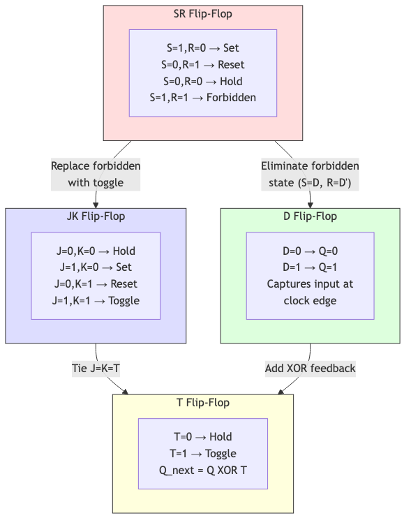
JK Flip-Flop: J=K=1 toggles; J=K=0 holds; J=1,K=0 sets; J=0,K=1 resets.
T Flip-Flop (Toggle): Q(next) = Q ⊕ T. When T=1, toggles each clock edge. Used for counters.
Relationship: D FF with feedback XOR = T FF. D FF is the most versatile.
Registers
A register is a group of flip-flops sharing a common clock, storing a multi-bit value.
n-bit register: n D flip-flops. Stores an n-bit word. Loaded on clock edge when LOAD is active.
Shift Registers
Data shifts one position per clock cycle.
Types:
- SISO (Serial-In, Serial-Out): Data enters and exits one bit at a time.
- SIPO (Serial-In, Parallel-Out): Serial input, all bits available at once.
- PISO (Parallel-In, Serial-Out): Load all bits, shift out serially.
- PIPO (Parallel-In, Parallel-Out): Essentially a register with shift capability.
Bidirectional shift register: Can shift left or right.
Applications: Serial communication (UART, SPI), CRC computation, pseudo-random number generation (LFSR), delay lines.
Linear Feedback Shift Register (LFSR)
A shift register with feedback XOR from selected taps.
┌──────────────────────────┐
│                          │
└──XOR──[D₃]──[D₂]──[D₁]──[D₀]──→ output
         ↑                  ↑
         └──────────────────┘ (tap)
With the right tap positions (primitive polynomial), cycles through all 2ⁿ-1 non-zero states. Used for pseudo-random number generation, scrambling, CRC computation.
Counters
Asynchronous (Ripple) Counter
Each flip-flop's clock is driven by the previous flip-flop's output.
Advantages: Simple design. Disadvantages: Accumulated delay — outputs don't change simultaneously (glitching). Not suitable for high-speed or when outputs are sampled simultaneously.
Synchronous Counter
All flip-flops share the same clock. Next-state logic ensures correct simultaneous transitions.
Binary up counter: T flip-flops with enable chains.
T₀ = 1            (always toggles)
T₁ = Q₀           (toggle when Q₀ = 1)
T₂ = Q₀ · Q₁      (toggle when Q₀Q₁ = 11)
T₃ = Q₀ · Q₁ · Q₂  (toggle when Q₀Q₁Q₂ = 111)
Modulo-N counter: Counts 0 to N-1, then wraps. Add reset logic when count reaches N-1.
Ring Counter
One-hot shift register. N flip-flops give N states. Simple but inefficient (only N states from N flip-flops vs 2ⁿ for binary).
Johnson (Twisted Ring) Counter
Complement of the last bit feeds back to the first. 2N states from N flip-flops. No glitches on state decoding.
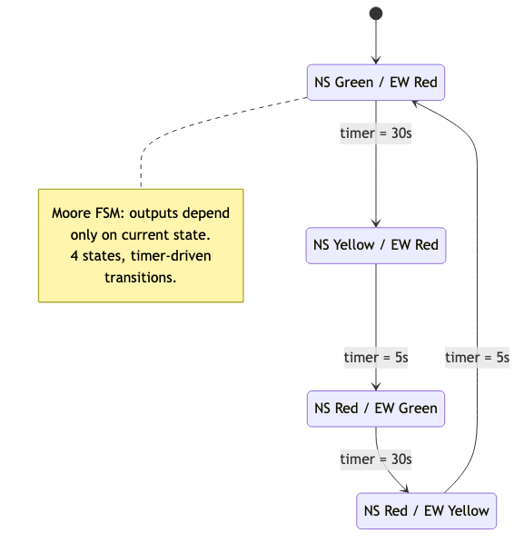
Finite State Machines (FSMs)
The general model for sequential circuits.
Mealy Machine
Output depends on current state AND current input.
Output = h(state, input)
Next state = f(state, input)
Outputs change asynchronously with inputs (can produce glitches). Typically responds one clock cycle faster than Moore.
Moore Machine
Output depends only on current state.
Output = g(state)
Next state = f(state, input)
Outputs are synchronous (change only at clock edges). Glitch-free. More states may be needed than Mealy.
FSM Design Procedure
- State diagram: Draw states (circles) and transitions (arrows with input/output labels).
- State table: List all states, inputs, next states, and outputs.
- State minimization: Merge equivalent states (same output and transitions to equivalent states).
- State encoding: Assign binary codes to states.
- Next-state logic: Derive combinational logic for flip-flop inputs.
- Output logic: Derive combinational logic for outputs.
State Minimization
Two states are equivalent if they produce the same output for all input sequences.
Implication table method: Mark pairs of states as distinguishable. Iterate until no more changes.
Partition refinement: Start with output-based partition. Refine by next-state behavior.
State Encoding
| Encoding | States | Bits per state | Advantages |
|---|---|---|---|
| Binary | Sequential | ⌈log₂ n⌉ | Minimum flip-flops |
| One-hot | One bit per state | n | Fast (simple next-state logic), fewer gates |
| Gray | Adjacent differ by 1 | ⌈log₂ n⌉ | Reduces switching, good for async interfaces |
FPGAs: One-hot is usually preferred (fast, logic cells are cheap). ASICs: Binary or optimized encoding (logic optimization tools choose).
Timing Analysis
Setup Time Constraint
For a flip-flop to correctly capture data, the combinational logic between two flip-flops must settle within one clock period:
tCLK ≥ tCQ + t_comb_max + tsu
where t_comb_max is the worst-case combinational delay.
Maximum clock frequency: f_max = 1 / (tCQ + t_comb_max + tsu).
Hold Time Constraint
Data must not change too quickly after the clock edge:
tCQ + t_comb_min ≥ thd
where t_comb_min is the minimum combinational delay.
Hold violations can't be fixed by slowing the clock — they require adding delay (buffer insertion).
Applications in CS
- Processor design: Pipeline registers, register files, program counter — all sequential.
- Memory: SRAM uses latches/flip-flops. Register files store processor state.
- Communication: UARTs use shift registers. Serial protocols (SPI, I2C) are FSMs.
- Control logic: Instruction decoders, cache controllers, bus arbiters — all FSMs.
- Counters: Performance counters, timer/watchdog, address generators.
- Protocol implementations: USB, PCIe, Ethernet — complex FSMs with many states.
- DSP: FIR filters use shift registers and adders. Accumulators use registers.